
 English
 French
Amorphous and polymorphous silicon
Thin film silicon coating by PECVD* from silane (SiH4) :
- A moderate temperature process 150-250°C
- High quality thin films are produced : hydrognated amorphous silicon, polymorphous, microcristalline, doped or intrinsic, silicon-carbon and silicon-germanium alloys …
- Necessary to get semiconducting properties, hydrogen is naturally incorporated by this technique
- It is self-cleaning by plasma etching of the reactors
* PECVD = Plasma Enhanced Chemical Vapor Deposition
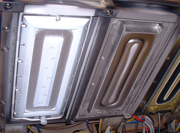
SOLEMS process for silicon p-i-n components : solar cells, modules and sensors.
| More in SOLEMS manufacturing process |
Available in SOLEMS on 300 x 300 mm sheets :
- a-Si:H intrinsic, p-type or n-type
- a-SiC:H p-type
- stacked layers p-i-n for example <1µm

Apply to us for any request.
Metallic coatings
for metallic coatings is :
- A low temperature process (< 80°C) compatible with many substrates
- A high speed coating
- Very energetic and dense
- Compatible with lots of metallic materials
Available in SOLEMS :
- Aluminium / Ti 1%
- Nickel
Laser patterning
Patterning, etching, isolation of conductive thin films, grooves in silicon layers for contacting …
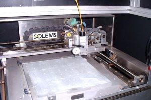
4 etching-lasers are available in SOLEMS :
- 2 YAG 1.064µm lasers with Q-switch (pulsed lasers) supplying short pulses of power for selective etching of oxides layers : SnO2, ITO, ZnO …etc…
- 2 double-frequency YAG lasers (532nm) also pulsed for silicon films etching.
The optical fiber driving the laser power is placed on a X-Y table moving tool. The patterning drawn on the thin films is therefore entirely programmable.
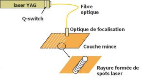
It is a sublimation process : the material is removed from its substrate, directly transformed into vapor by the heat generated by the laser pulse. By tuning the laser intensity, the Q-switch frequency, the tool speed, it is possible to get either a continuous isolation line, or separate spots, for example to perform a top-bottom electrical contact through a layer.
This technique is namely used to :
- isolate conductive areas on a TCO (transparent conducting oxide)
- cut very hard ceramic layers without contact
- ensure the series connection of neighbouring cells on a thin film solar cell or module by contacting metal (-) and TCO (+) of the 2 cells through the holes made by laser in the silicon layer
Concerning the use of this process in SOLEMS products, see :
| SOLEMS manufacturing process |
Apply to us for any request.