
SOLEMS thin film technology devoted to solar cells and modules production is «thin film silicon » or « amorphous silicon » technology, single junction.
The benefits of this design :
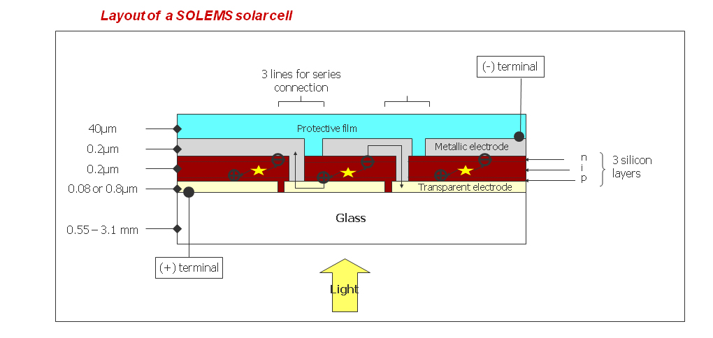
- Amorphous silicon light-absorption coefficient quite high over the solar spectrum; therefore only a thin film is necessary (< 1 micrometer thick).
- The films can easily be patterned (for example by laser, see below), making easy the series connection between neighboring cells, avoiding bus soldering
- Very low amount of silicon material used
- Excellent conversion efficiency under low illumination light source
See “solar cells” -> fiche produit
Thin film production
In SOLEMS two main production processes of thin film production, among vacuum technologies are available :
- PECVD « Plasma Enhanced Chemical Vapor Deposition » ou Dépôt chimique en phase vapeur assisté par plasma
and
- la PVD « Physical Vapor Deposition », more precisely « Magnetron supttering »
PECVD process
This technique is dedicated to the production of thin film materials on a substrate, from a gas precursor, in a reactor pumped down to secondary vacuum. For the deposition of silicon and silicon-based coatings, the main precursor is Silane (SiH4). It is broken down in a plasma * created inside the reactor. This plasma is produced by an electrical RF discharge (13.56 MHz) between 2 electrodes. Other gases are added in order to produce alloys: for example CH4 for SiC compounds, B2H6 for p-doped silicon, and PH3 for n-doped. The substrate sheets placed inside the reactor are heated up to 150-200°C prior to deposition. Then the stack of the different layers p-i-n necessary to create a photovoltaic junction is made during a single process by changing the gas mixture, without stopping the plasma.
* a plasma is a ionized medium made up of electrons, ions, photons and neutral species, in the fundamental or excited state. It is created by a discharge. The species are created by collision of the gas molecules with fast electrons (primary reactions) and between them when they are reactive (secondary reactions).

Magnetron sputtering
This process differs from the PECVD by the fact that the source of the thin film material is solid (the target) instead of gaseous. A neutral gas, generally Argon, is introduced inside the reactor, previously pumped down to secondary vacuum. Putting a negative voltage on the target (cathode) against the walls of the machine produces a plasma. The negative voltage attracts the Ar+ ions towards the target, ejecting some atoms from the target (“sputtering”) that will condense on the substrate. The thin film forms according to several mechanisms depending on binding forces and collisions. For a better sputtering efficiency, a magnetic confinement of the electrons is made by magnets located on North-South top of the target.
This technique is used for metallic films, oxides and nitrides. The low temperature if the process (< 80°C) makes it compatible with polymer substrates.
In SOLEMS it is used to produce Aluminum and Nickel films as solar cells and modules back contact and also to produce ITO films (Indium-tin-oxide) as substrates or special applications.

The production of oxides instead of metallic films by PVD is done by addition of Oxygen to the Argon gas. It is the reactive sputtering technique. The coatings stoechiometry is tuned by oxygen partial pressure essentially. Sometimes an oxide is formed at the surface of the target first. The reactive gas (here oxygen) reacts with the surfaces located inside the reactor (target, substrate, walls) and modifies the electrical characteristics of the discharge.

Thin film patterning
SOLEMS has 4 ablation lasers :
- 2 YAG 1.064µm lasers with a Q-switch (pulsed lasers) delivering ultra-short pulses for the selective ablation of oxide layers : FTO, ITO, ZnO…
- 2 YAG lasers with a double frequency (532nm) also pulsed, dedicated to the ablation of silicion and silicon-based layers.
The energy is guided in an optical fiber placed on a scribing X-Y table, therefore compatible with any patterning design.
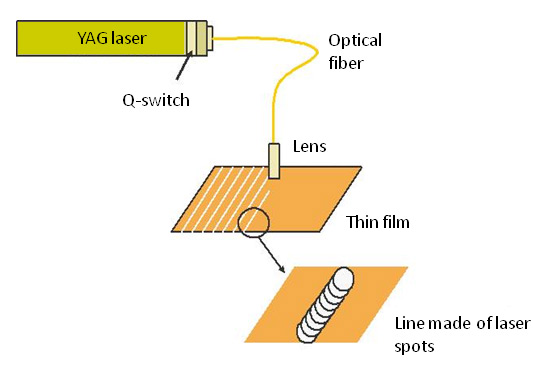
It s an ablation process because the layers are converted from solid to vapor state directly by sublimation thanks to the laser energy. By tuning the scanning speed and the Q-switch frequency, a line (for isolation) or separate spots (for contacting) are obtained.
This technique is used to :
- isolate some conductive areas on an conductive substrate
- cut very hard coatings without mechanical action
- Open apertures in a silicon thin film in order to create a contact passing through between the top and bottom (for series connections).